Apple is set to give its Ray-Ban Meta smart glasses a run for their money by launching a superior competitor, replete with a more premium build and greater design versatility, according to the latest Power On newsletter from Bloomberg’s Mark Gurman.
Mark Gurman today revealed that Apple’s upcoming screenless smart glasses will likely launch in early 2027, and feature an integrated camera, microphone and speaker, allowing wearers to interact via an improved version of its bespoke AI assistant, Siri.
The new camera-equipped smart glasses will be able to take photos and videos, sync with an iPhone for post-capture editing and sharing, handle phone calls, keep an eye on notifications, play music, and enable hands-free interaction via Siri.
The smart glasses will join Apple’s new lineup of AI-powered devices, including the camera-equipped AirPods Pro and AI pendant. All of these devices will leverage computer vision to interpret a user’s surroundings and provide contextual awareness directly to Siri and Apple Intelligence, enabling features like better turn-by-turn map directions and visual reminders.
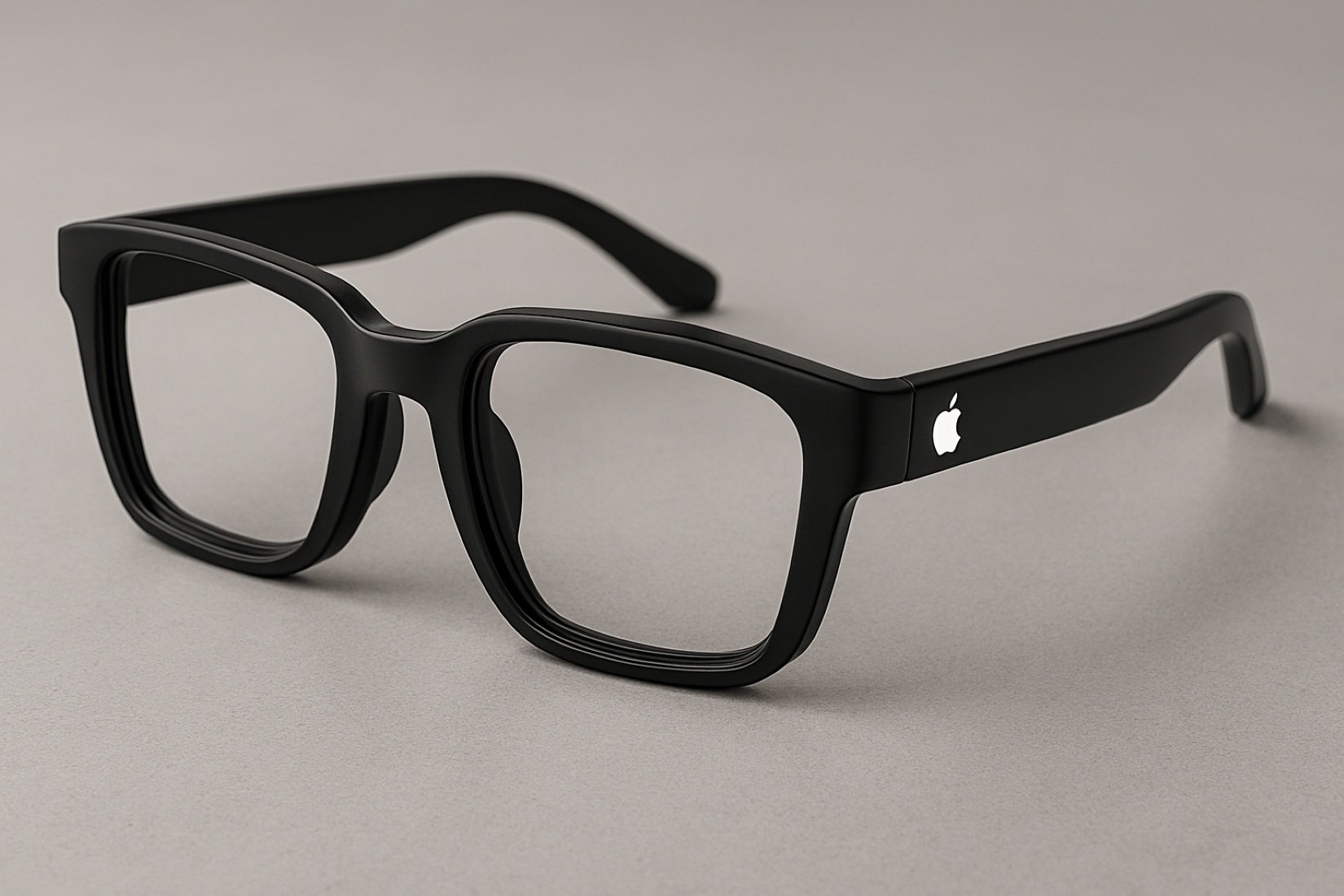
Interestingly, Apple plans to create a major difference between its smart glasses and the Meta glasses by implementing tight, utility-packed integration with the iPhone. Additionally, Apple appears to be opting for a more premium acetate frame for its smart glasses, along with a number of color and design options:
- Large rectangular frames similar to Ray-Ban Wayfarers.
- The sleeker rectangular design mimics the glasses worn by Apple Chief Executive Officer Tim Cook.
- Larger oval or circle frames.
- Smaller, smoother oval or circle options.
- The camera system may use a vertically oriented oval lens.
- Color choices include black, navy blue and light brown.
Gurman concluded by noting:
“Despite Meta’s early lead and Google’s lead in the larger Android ecosystem, Apple’s strengths – its brand, in-house chips, giant retail presence and deep iPhone integration – position it well to compete. If executed well with a functional Siri, the glasses could follow a similar trajectory to the Apple Watch: not first to market, but ultimately dominant.”
Elsewhere, Omdia predicts Apple will launch its own AR smart glasses – equipped with dual 0.6-inch OLEDoS displays – only in 2028, a few months after Meta might launch its own competitive offering.
For those who may not be aware, OLEDoS, also called Micro-OLED display technology, mounts Organic Light Emitting Diodes (OLEDs) directly onto a single crystal silicon wafer substrate. Unlike traditional OLED displays used in smartphones or TVs that are made with glass or plastic bases, OLEDoS leverages semiconductor manufacturing processes to achieve miniaturization and extreme performance, resulting in ultra-high pixel densities and better power consumption profiles, especially because the circuitry is integrated directly into the silicon backplane using CMOS technology.

About the author: Writing is one of my undeniable passions. Over the past six years, he has written more than 2,200 different articles on finance and technology-related topics, spanning nearly 1 million words. And he has been a member of Wcctech’s mobile team since 2025. As an alumnus of the University of Toronto, Rotman Commerce Program, I bring nuance, deep knowledge and a unique perspective to every topic I cover. When I’m not writing, I travel the world, exploring hidden gems and restaurants as an aspiring food connoisseur.
Follow Wccftech on Google to get more of our news coverage in your feed.
PakarPBN
A Private Blog Network (PBN) is a collection of websites that are controlled by a single individual or organization and used primarily to build backlinks to a “money site” in order to influence its ranking in search engines such as Google. The core idea behind a PBN is based on the importance of backlinks in Google’s ranking algorithm. Since Google views backlinks as signals of authority and trust, some website owners attempt to artificially create these signals through a controlled network of sites.
In a typical PBN setup, the owner acquires expired or aged domains that already have existing authority, backlinks, and history. These domains are rebuilt with new content and hosted separately, often using different IP addresses, hosting providers, themes, and ownership details to make them appear unrelated. Within the content published on these sites, links are strategically placed that point to the main website the owner wants to rank higher. By doing this, the owner attempts to pass link equity (also known as “link juice”) from the PBN sites to the target website.
The purpose of a PBN is to give the impression that the target website is naturally earning links from multiple independent sources. If done effectively, this can temporarily improve keyword rankings, increase organic visibility, and drive more traffic from search results.